
Table of Contents
Benefits of Using Layer HDI Technology in PCB Design
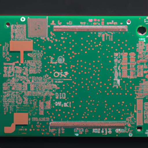
Printed circuit Boards (PCBs) are an essential component in electronic devices, serving as the foundation for connecting various electronic components. As technology advances, the demand for smaller, faster, and more reliable PCBs has increased. This has led to the development of high-density interconnect (HDI) technology, which offers numerous benefits for PCB design.
One of the key advantages of using layer HDI technology in PCB design is the ability to achieve higher component density. Traditional PCBs have limitations in terms of the number of components that can be placed on a single board due to space constraints. However, with HDI technology, designers can stack multiple layers of components on top of each other, allowing for a higher component density in a smaller footprint.
In addition to higher component density, layer HDI technology also offers improved signal integrity. By reducing the length of signal traces and minimizing signal interference, HDI technology helps to ensure that signals are transmitted accurately and efficiently. This is particularly important in high-speed applications where signal integrity is critical for the overall performance of the electronic device.
Furthermore, layer HDI technology enables the use of advanced packaging techniques such as ball grid array (BGA) and chip-scale packaging. These packaging techniques allow for smaller and more compact components to be used, further reducing the overall size of the PCB. This is especially beneficial for portable electronic devices where space is limited and compactness is essential.
Another advantage of using layer HDI technology in PCB design is the ability to achieve better thermal management. By stacking components closer together, heat dissipation is improved, resulting in more efficient cooling of the electronic device. This is particularly important in high-power applications where heat generation can be a significant concern.
Moreover, layer HDI technology offers increased reliability and durability. By reducing the number of through-holes and vias, which are common points of failure in traditional PCBs, HDI technology helps to improve the overall reliability of the electronic device. This is crucial in applications where the PCB is subjected to harsh environmental conditions or high Levels of vibration.
Additionally, layer HDI technology allows for greater design flexibility. Designers have more freedom to place components in unconventional configurations, leading to more innovative and efficient PCB layouts. This flexibility also enables designers to meet the specific requirements of the electronic device, whether it be size constraints, performance specifications, or cost considerations.
In conclusion, layer HDI technology offers numerous benefits for PCB design, including higher component density, improved signal integrity, advanced packaging techniques, better thermal management, increased reliability, durability, and greater design flexibility. As technology continues to evolve, the demand for smaller, faster, and more reliable electronic devices will only continue to grow. By incorporating layer HDI technology into PCB design, designers can meet these demands and create cutting-edge electronic devices that push the boundaries of what is possible.